
Wafer prober
Contact us for a SweepMe! Pro trial license!
What type of measurements are related to wafer prober?
DC Electrical Characteristics These measurements involve assessing the DC behavior of semiconductor devices, such as voltage current (IV) characteristics, resistance, and leakage current.
AC Electrical Characteristics: Wafer probing also includes measurements of AC electrical parameters, such as capacitance, inductance, and frequency response, which are crucial for understanding the device's high-frequency performance.
Functional Testing: This involves applying specific input signals to the device under test and measuring the corresponding output signals to verify its functionality according to the intended design specifications.
Parametric Testing: Parametric testing involves measuring key parameters of semiconductor devices, such as threshold voltage, gain, saturation current, and breakdown voltage, to ensure they meet performance requirements.
Reliability Testing: Wafer probing may include reliability tests to evaluate the long-term stability and robustness of semiconductor devices under various operating conditions, including temperature and voltage stress.
Defect Detection: Wafer probing is also used for defect detection and characterization, where anomalies in device behavior or performance are identified and analyzed to determine their root causes and potential impact on device reliability and functionality.
Wafer Terminology and Organization for Wafer Prober Applications
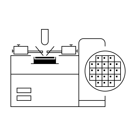
Wafer: A thin slice of semiconductor material (typically silicon, SiC, or GaN) that serves as the foundation for manufacturing integrated circuits (ICs). It can contain hundreds or even thousands of identical circuits or "chips."
Chip (Die): An individual integrated circuit fabricated on a wafer. Each chip represents a complete functional unit, like a microprocessor or memory device. The terms "chip" and "die" are often used interchangeably.
Subsite (Subdie): Within a complex chip, there might be further functional subdivisions called subsites or subdies. These represent smaller functional blocks or modules within the overall chip design.
Reticle: A high-precision mask used in the photolithography process to define circuit patterns on the wafer. Light shining through the patterned areas of the reticle creates the desired circuit features on the wafer surface.
Pads: These are metal contact areas on the periphery of a chip or subsite designed for electrical connection to the outside world. During wafer probing, these pads are the points where the tester makes contact with the circuitry using probes.
Wafer Organization:
Die Layout: The entire wafer surface is meticulously planned to accommodate a large number of identical chips or dies. This layout optimizes wafer utilization and minimizes wasted space.
Testing Considerations: Wafer prober compatibility is factored into the die layout. Special alignment marks and electrical test structures might be incorporated to facilitate automated probing and testing procedures. Test structures are often added between two dies. They can be used to check the process quality. When the wafer is splitted into single chips, they are destroyed, but can be used beforehand for checking the general wafer process quality by using standard devices like resistors, capacitors or transistors.
Dicing: After fabrication and testing, the wafer is diced into individual chips using a specialized saw. Each diced chip becomes a separate functional integrated circuit ready for packaging.
Types of Wafer Prober
Manual Wafer Prober: Require manual operation to load the wafer onto the chuck, align probes, and initiate testing. Common in research or low-volume testing.
Semiautomatic Wafer Prober: Combine manual loading with automated positioning and testing. Operators load wafers manually while the prober automates probe alignment and test execution, offering improved efficiency.
Automatic Wafer Prober: Fully automated systems for high-volume testing. Feature robotic wafer handling, automated alignment, and integrated test sequence execution, maximizing throughput in semiconductor manufacturing.
Vertical Wafer Prober: Orient wafers vertically during testing, leveraging gravity for consistent probe-device contact. Suitable for delicate structures and advanced semiconductor applications.
Horizontal Wafer Prober: Position wafers horizontally, providing easy access to the surface and probe manipulators. Versatile for various wafer sizes and testing needs.
In which application fields they are used
Integrated Circuit Manufacturing: Wafer probers ensure device functionality and reliability during manufacturing by testing individual devices on silicon wafers for defects and variations before assembly into integrated circuits.
Wafer-Level Testing: Wafer probers support efficient testing of multiple devices on a single wafer simultaneously, streamlining production processes and reducing costs.
Research and Development: In R&D settings, wafer probers characterize new materials, test novel device designs, and explore emerging technologies, providing insights for advancing semiconductor innovation.
Quality Control and Assurance: Wafer probers play a crucial role in quality control by identifying defects early in the manufacturing process, ensuring the production of high-quality products that meet performance standards.
Failure Analysis: Wafer probers are essential for diagnosing device failures and improving processes, contributing to enhanced product reliability and performance.
Product Characterization: Wafer probers facilitate comprehensive testing of semiconductor devices under various conditions, providing valuable data for optimizing device designs and meeting customer requirements.
What are important specifications?
Wafer Size Compatibility: Wafer probers may support wafer sizes ranging from 2 inches to 12 inches or more, depending on the model.
Chuck Type: Vacuum chucks typically provide uniform suction across the wafer surface, ensuring secure wafer positioning during testing.
Probing System: A wafer prober may have a probing capacity of 1,000 or more probes, with a pitch (distance between probes) ranging from 50 to 500 micrometers.
Accuracy and Precision: Wafer probers can offer positioning accuracy ranging from 1 to 10 micrometers (µm) and precision within a few nanometers (nm).
Automation Features: Automatic wafer probers can handle hundreds of wafers per hour, depending on the specific model and configuration.
Throughput: Throughput rates for wafer probers vary widely but can range from 50 to 300 wafers per hour for high-volume production environments.
Environmental Control: Wafer probers may offer temperature control within a range of ±0.1 to ±1 degree Celsius and humidity control within a range of 30% to 70% relative humidity.
Wafer Prober and SweepMe!
Instrument Control: SweepMe! can interface with wafer probers to control their operation, including wafer loading, probe alignment, and test execution. Through SweepMe!, users can send commands to the prober and receive feedback to automate testing processes.
Data Acquisition: Wafer probers generate large amounts of data during semiconductor testing, including electrical measurements and device characteristics. SweepMe! facilitates data acquisition from the prober's measurement systems, allowing users to collect, analyze, and visualize test data in real-time or post-processing.
Automation: SweepMe! enables the automation of complex testing sequences and procedures on wafer probers. Users can develop custom test scripts and routines in SweepMe! to automate repetitive tasks, optimize testing throughput, and improve overall efficiency in semiconductor manufacturing.
Integration with Test Equipment: In semiconductor testing environments, SweepMe! serves as a central platform for integrating various test equipment, including wafer probers, prober manipulators, test instruments (such as oscilloscopes and multimeters), and analysis tools. SweepMe!'s modular architecture and compatibility with industry-standard communication protocols facilitate seamless integration and interoperability among different testing components.
Customization and Flexibility: SweepMe! provides a highly flexible and customizable development environment for designing tailored solutions for wafer-probing applications. Users can create user-friendly graphical interfaces, develop custom measurement algorithms, and implement advanced data analysis techniques to meet specific testing requirements and address unique challenges in semiconductor testing.
SweepMe! in practice
Wafer prober in real measurement setups
Your partner for the integration
Wafer prober support and integration
Built from real lab practice
SweepMe! was founded in 2018 by Dr. Axel Fischer and Dr. Felix Kaschura after their PhDs in applied physics. Since then the company has grown into a service oriented partner for industry and research alike, and more than 100 companies and research institutes run their measurements with SweepMe! today. We know what a measurement setup has to deliver, we make the technology work for you, and we understand the science behind your data.